- 您现在的位置:买卖IC网 > Sheet目录325 > FAN5341UMPX (Fairchild Semiconductor)IC LED DVR BOOST W/DIO 6-ULMP
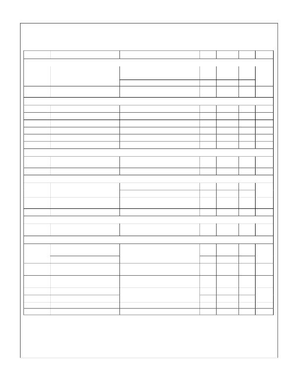
Electrical Specifications
V IN = 2.7V to 5.5V and T A = -40°C to +85°C unless otherwise noted. Typical values are at T A = 25°C and V IN = 3.6V.
Symbol
Parameter
Conditions
Min.
Typ.
Max.
Units
Power Supplies
I SD
Shutdown Supply Current
EN = GND, V IN = 3.6V
0.30
0.75
μ A
V UVLO
Under-Voltage Lockout
Threshold
V IN Rising
V IN Falling
2.10
1.90
2.35
2.15
2.60
2.40
V
V UVHYST
Under-Voltage Lockout
Hysteresis
250
mV
EN: Enable Pin
V IH
V IL
HIGH-Level Input Voltage
LOW-Level Input Voltage
1.2
0.4
V
V
R EN
EN Pull-Down Resistance
200
300
400
k Ω
T LO
T HI
T SD
EN Low Time for Dimming
Time Delay Between Steps
EN Low, Shutdown Pulse Width
V IN = 3.6V; See Figure 14
V IN = 3.6V; See Figure 14
V IN = 3.6V; from Falling Edge of EN
0.5
0.5
1
300
μs
μs
ms
Feedback and Reference
V FB
I FB
Feedback Voltage
Feedback Input Current
I LED = 20mA from -40°C to +85°C,
2.7V ≤ V IN ≤ 5.5V
V FB = 253mV
240
253
0.1
266
1.0
mV
μ A
Power Outputs
R DS(ON)_Q1
Boost Switch On-Resistance
V IN = 3.6V, I SW = 100mA
V IN = 2.7V, I SW = 100mA
600
650
m Ω
SW Node Leakage
I SW(OFF)
I LIM-PK
(1)
Boost Switch Peak Current Limit
EN = 0, V IN = V SW = V OUT = 5.5V,
V LED = 0
V IN = 3.6V
0.1
750
2.0
μ A
mA
Oscillator
f SW
Boost Regulator Switching
Frequency
1.0
1.2
1.4
MHz
Output and Protection
V OVP
Boost Output Over-Voltage
Protection
18.0
18.9
21.0
V
OVP Hysteresis
0.8
Maximum Boost Duty Cycle
Minimum Boost Duty Cycle
V TLSC
V THSC
D MAX
D MIN
T TSD
T HYS
V OUT Short Circuit Detection
Threshold
V OUT Short Circuit Detection
Threshold
(2,3)
(2,3)
Thermal Shutdown
Thermal Shutdown Hysteresis
V OUT Falling
V OUT Rising
85
V IN – 1.4
V IN – 1.2
150
35
20
V
V
%
°C
°C
Notes:
1. SW leakage current includes the leakage current of 2 internal switches; SW to GND and SW to VOUT .
2. Not tested in production and guaranteed by design.
3. Application should guarantee that minimum and maximum duty cycle should fall between 20-85% to meet the specified
range.
? 2009 Fairchild Semiconductor Corporation
FAN5341 ? Rev. 1.0.1
5
www.fairchildsemi.com
发布紧急采购,3分钟左右您将得到回复。
相关PDF资料
FAN5343UMPX
IC LED DVR 6LED 500MW 6UMLP
FAN5345S30X
IC LED DVR ASYNC BOOST 30V 6SSOT
FAN5346S30X
IC LED DVR ASYNC SER BOOST 6SSOT
FAN53540UCX
IC REG SYNC BUCK 5A 20WLCSP
FAN5626LX
IC LED DVR 6CH INTERFACE 10-UMLP
FAN5640S7X
IC LED DRIVER DUAL CC SC70-6
FAN5646S700X
IC LED DRIVER BLINKER SC70-5
FAN5701UMP30X
IC LED DVR MULTI 30MA 16-UMLP
相关代理商/技术参数
FAN5343
制造商:FAIRCHILD 制造商全称:Fairchild Semiconductor 功能描述:6-LED Series Boost LED Driver with Integrated Schottky Diode and Single-Wire Digital Interface
FAN5343UMPX
功能描述:LED照明驱动器 6-LED BOOST LED DRVR
RoHS:否 制造商:STMicroelectronics 输入电压:11.5 V to 23 V 工作频率: 最大电源电流:1.7 mA 输出电流: 最大工作温度: 安装风格:SMD/SMT 封装 / 箱体:SO-16N
FAN5345
制造商:FAIRCHILD 制造商全称:Fairchild Semiconductor 功能描述:Series Boost LED Driver with Single-Wire Digital Interface
FAN5345S20X
功能描述:LED照明驱动器 Async Series Driver SingleWire Dig Intfc RoHS:否 制造商:STMicroelectronics 输入电压:11.5 V to 23 V 工作频率: 最大电源电流:1.7 mA 输出电流: 最大工作温度: 安装风格:SMD/SMT 封装 / 箱体:SO-16N
FAN5345S30X
功能描述:LED照明驱动器 Async Series Driver SingleWire Dig Intfc RoHS:否 制造商:STMicroelectronics 输入电压:11.5 V to 23 V 工作频率: 最大电源电流:1.7 mA 输出电流: 最大工作温度: 安装风格:SMD/SMT 封装 / 箱体:SO-16N
FAN5346
制造商:FAIRCHILD 制造商全称:Fairchild Semiconductor 功能描述:Series Boost LED Driver with PWM Dimming Interface
FAN5346S20X
功能描述:LED照明驱动器 Async Series Driver ANLG PWM DIM Intfc RoHS:否 制造商:STMicroelectronics 输入电压:11.5 V to 23 V 工作频率: 最大电源电流:1.7 mA 输出电流: 最大工作温度: 安装风格:SMD/SMT 封装 / 箱体:SO-16N
FAN5346S30X
功能描述:LED照明驱动器 Async Series Driver ANLG PWM DIM Intfc RoHS:否 制造商:STMicroelectronics 输入电压:11.5 V to 23 V 工作频率: 最大电源电流:1.7 mA 输出电流: 最大工作温度: 安装风格:SMD/SMT 封装 / 箱体:SO-16N
